Downloaded 2,282 times
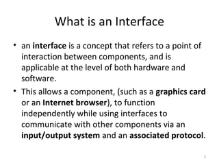
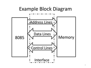
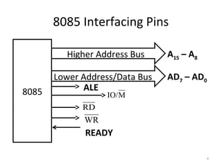
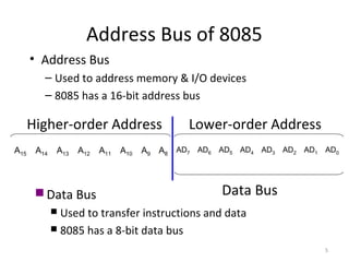
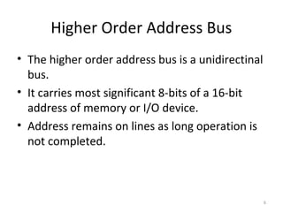
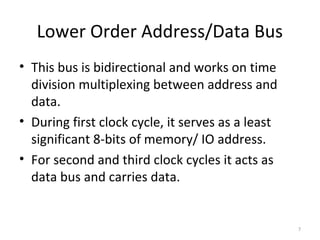
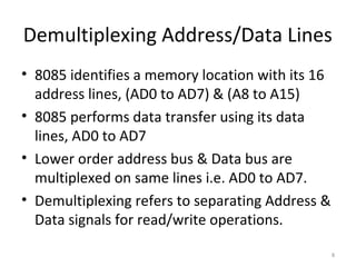
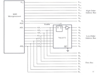
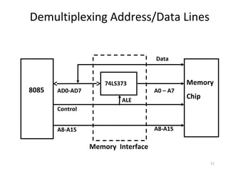
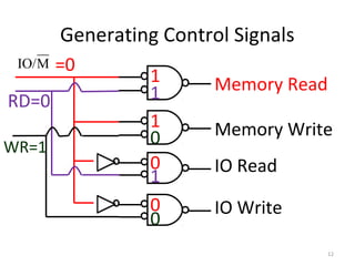
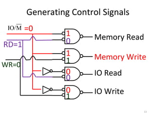
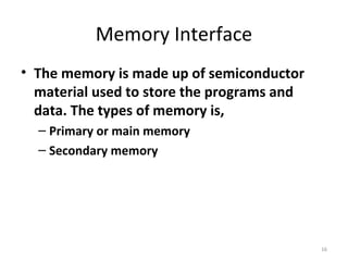
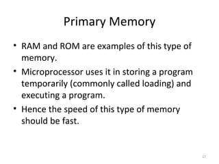
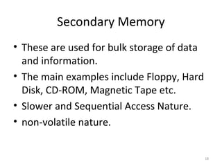
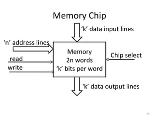
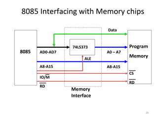


This document discusses memory and I/O interfacing with the 8085 microprocessor. It defines interfaces as points of interaction between components that allow communication. Memory interfacing requires address decoding and multiplexing of address and data lines. I/O devices can be interfaced either through memory mapping or I/O mapping. Common memory types include RAM, ROM, SRAM and DRAM. RAM can be static or dynamic. ROM includes PROM, EPROM and EEPROM. A stack is a reserved part of memory used to temporarily store information during program execution.


![INTERFACING2 [Autosaved] interfacing in Computer system](https://cdn.slidesharecdn.com/ss_thumbnails/interfacing2autosaved-250404124048-193f189f-thumbnail.jpg?width=640&height=640&fit=bounds)